English
 中文简体
中文简体 русский
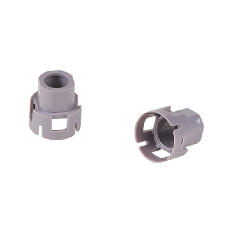
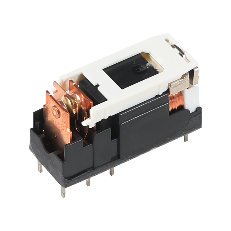
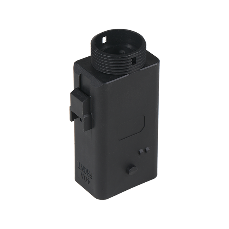
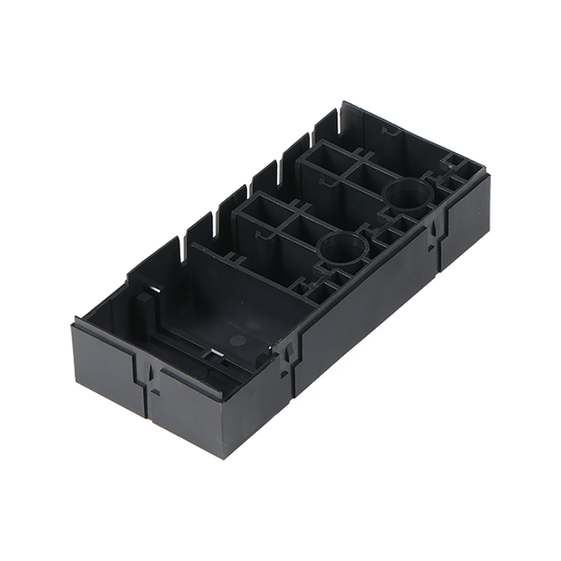
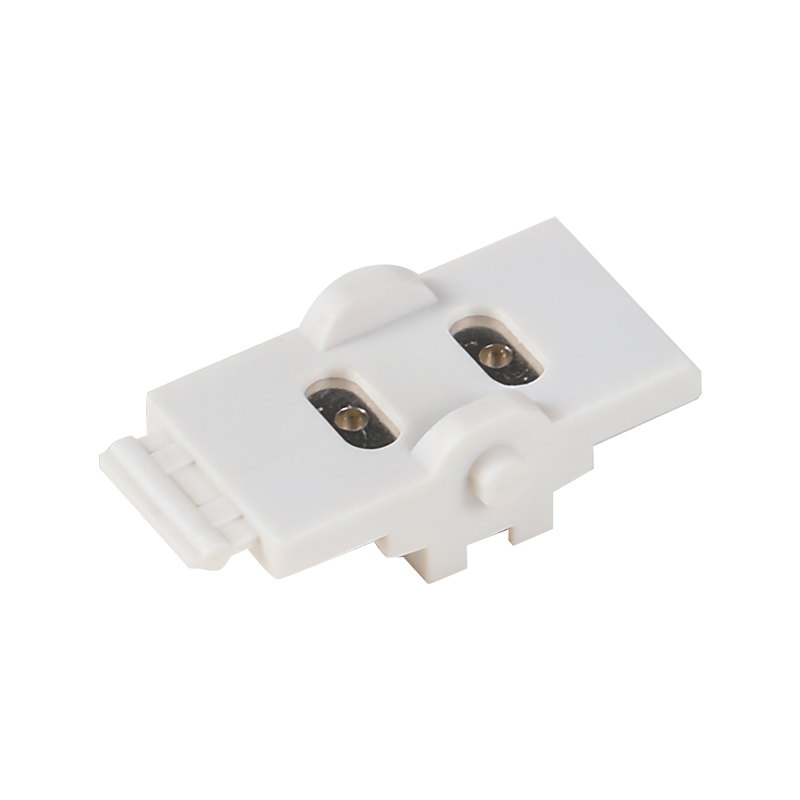
Design pcb enclosure with connector Manufacturer
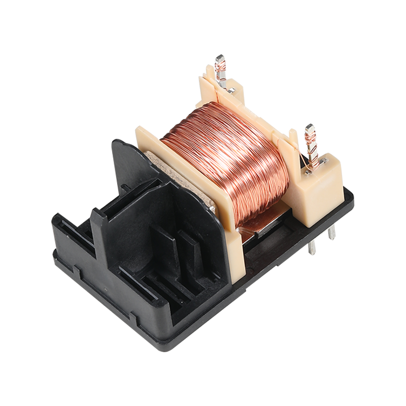
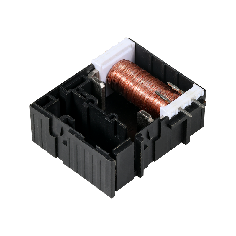
The connection between a printed circuit board (PCB) and its enclosure is crucial for both functionality and protection. When we think about a PCB enclosure with connector, we envision a seamless integration that not only safeguards the delicate components inside but also facilitates efficient connectivity. The design of a PCB enclosure with connector is not merely a matter of aesthetics; it is a fundamental aspect that influences the performance and reliability of electronic devices.
As we delve into the intricacies of how a PCB enclosure with connector operates, we must consider the grounding techniques employed. Grounding is essential in any electronic system, and it can be categorized into two primary methods: single-point grounding and multi-point grounding. Each method has its own set of advantages and disadvantages, which can significantly impact the overall performance of our connector.
Single-point grounding is often favored for its simplicity. In this approach, all ground connections converge at a single point, creating a common reference for the entire system. This method minimizes the risk of ground loops, which can introduce noise and interference into our circuits. When we incorporate a PCB enclosure with connector designed for single-point grounding, we can ensure that our signals remain clean and reliable. However, this method is not without its drawbacks. In larger systems or those operating at higher frequencies, single-point grounding can lead to potential issues with signal integrity, as the distance from the ground reference can introduce variations in voltage levels.
On the other hand, multi-point grounding offers a more robust solution for complex systems. By establishing multiple grounding points throughout the PCB enclosure with connector, we can create parallel paths for the return current. This approach enhances the system's ability to handle high-frequency signals and reduces the risk of electromagnetic interference (EMI). When we design a PCB enclosure with connector that utilizes multi-point grounding, we are essentially fortifying our circuit against the unpredictable nature of electrical noise. However, this method can complicate the design process, as it requires careful planning to avoid ground loops and ensure that all grounding points are effectively connected.
As we explore the relationship between our PCB enclosure with connector and grounding techniques, it becomes evident that the choice of method depends on the specific requirements of our application. For instance, in a compact device where space is at a premium, a well-designed PCB enclosure with connector that employs single-point grounding may suffice. Conversely, in a high-performance application where signal integrity is paramount, a multi-point grounding strategy within the PCB enclosure with connector could be the key to success.
Moreover, the materials used in the construction of our enclosure with connector play a significant role in its effectiveness. Choosing materials that provide adequate shielding against EMI while maintaining thermal management is essential. A well-designed PCB enclosure with connector not only protects the internal components but also enhances the overall performance of the device by ensuring that heat dissipation is managed effectively.
The connection between a PCB and its enclosure is a critical aspect of electronic design. By understanding the implications of grounding techniques and the importance of a well-constructed PCB enclosure with connector, we can create devices that are not only functional but also reliable. Whether we opt for single-point or multi-point grounding, the design of our PCB enclosure with connector must be approached with careful consideration of the specific needs of our application. Ultimately, the goal is to achieve a harmonious balance between protection, performance, and connectivity, ensuring that our electronic devices can thrive in an increasingly complex technological landscape.